New process layers uniform ScAlN on 3D surfaces
Scandium aluminum nitride can now be integrated into high-voltage, high-frequency or piezoelectric devices with plasma-enhanced atomic layer deposition.
Scandium aluminum nitride can now be integrated into high-voltage, high-frequency or piezoelectric devices with plasma-enhanced atomic layer deposition.
Experts
The first demonstration of scandium aluminum nitride (ScAlN) thin films grown by plasma-enhanced atomic layer deposition expands application to complex 3D structures, according to a University of Michigan study published in Applied Physics Letters and funded by the Army Research Office.
Conventional methods—sputtering and epitaxy—can only layer ScAlN on flat surfaces, limiting application as most devices have complex geometries. The new method allows precise control over ScAlN thickness, scandium content and uniformity at lower processing temperatures.
“This approach makes high-performance ScAlN more accessible to research labs and paves the way for integrating it into advanced devices that were previously out of reach,” said Md Mehedi Hasan Tanim, a doctoral student of electrical and computer engineering and lead author of the study.
ScAlN’s ability to generate electricity when mechanically stressed—known as a piezoelectric effect—has been investigated for use in wearable energy harvesters capable of converting mechanical motion, such as walking or body movement, into usable electrical power
As an ultra-wide bandgap material, ScAlN can also improve high-power devices like EV power converters, as it can handle high voltages without breaking down. High-frequency devices, like filters or amplifiers for future 5G or 6G cell phones, can also leverage ScAlN’s superior piezoelectric and acoustic properties—as well as high current handling capability, which allows better signal quality and higher data rates.
Despite the worldwide interest in ScAlN, it has remained unknown if it can be grown or synthesized using plasma-enhanced atomic layer deposition.
Plasma-enhanced atomic layer deposition starts by sending the gas-phase material to be deposited into a chamber containing the target surface. Some of the material sticks to the surface, and the rest is swept away with an inert gas. That gas, in turn, is swept out by the gas that forms the plasma, which reacts with the layer to set it. To create ScAlN thin films, researchers use a supercycle growth approach—fine tuning the timing and ratio of aluminum nitride (AlN) and scandium nitride (ScN) layers—within a temperature range of 225 to 250 C.
“Atomic layer deposition of ScAlN is like spray-painting at the atomic scale. Each pass lays down an ultrathin, self-limiting coat, and by repeating the process we achieve a precise, uniform film,” said Zetian Mi, the Pallab K. Bhattacharya Collegiate Professor of Engineering at U-M and corresponding author of the study.
Thin films were grown on a gallium nitride/sapphire substrate—another material well-suited for high-power, high-frequency or piezoelectric devices. Electron microscopy confirmed the new method allows precise scandium composition control (0–25%) while maintaining atomically smooth surfaces.
Further, each element was evenly mixed rather than clumped, and there were few defects at the boundary between the thin film and substrate. Both properties ensure the ease of integration into existing gallium nitride devices.
Piezoelectric strength in ScAlN grown with plasma-enhanced atomic layer deposition matched those produced with conventional sputtering or epitaxy, proving piezoelectric properties persist even when layered in different geometries.
“Going forward, we plan to explore integrating ALD-grown ScAlN into device prototypes to leverage its unique material properties and scalable processing,” said Mi.
Zetian Mi is also a professor of electrical and computer engineering and materials science and engineering at U-M.

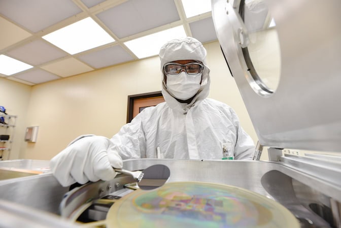
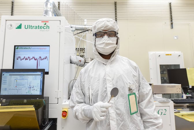
The technique was developed in the Lurie Nanofabrication Facility and studied at the Michigan Center for Materials Characterization, both of which are operated and maintained with support from indirect cost allocations in federal grants.
This research was funded in part by the Army Research Office (W911NF-24-2-0210).