Nanoscale hotspots in OLEDs may shorten their lifespans in phones, TVs
Concentrated rivers of current create flickering hotspots in conventional amorphous OLEDs, but crystalline designs may not have this problem.
Concentrated rivers of current create flickering hotspots in conventional amorphous OLEDs, but crystalline designs may not have this problem.
The pixels in phone screens and other OLED displays appear to provide a uniform glow, but a team of University of Michigan Engineering researchers has discovered the light actually originates from nanoscale hotspots, some of which flicker.
This might be hurting device lifespans.
“If some areas are carrying more current than others, they’re likely to burn out faster,” said Steve Forrest, the Peter A. Franken Distinguished University Professor of Engineering and one of the senior authors of the study in Nature Photonics. “This phenomenon could affect the reliability and performance of devices, such as the efficiency of solar cells or the charge mobility in transistors. It permeates everything that’s organic, so it’s very fundamental but also very practical.”
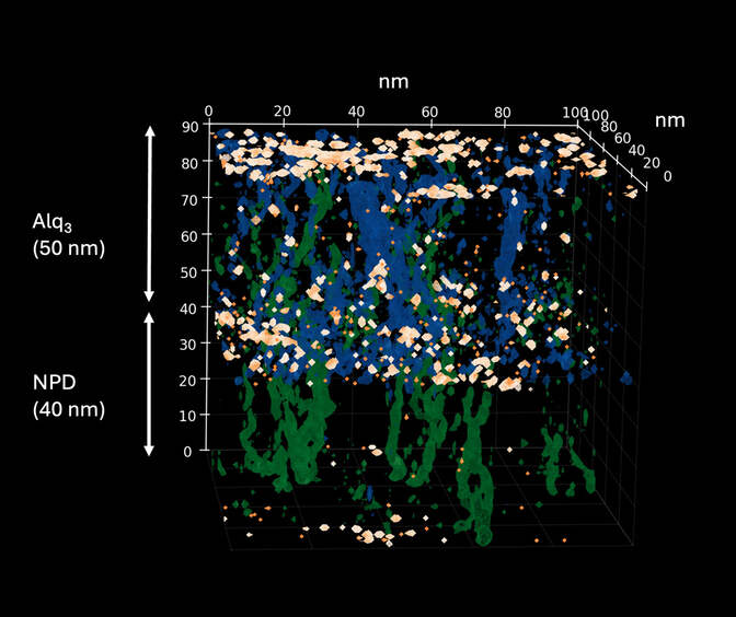
The team also suggests a fix for organic, or carbon-based, electronics: crystalline structures, rather than the typical amorphous structure, may last longer. The research was supported by the U.S. Department of Energy and Universal Display Corp.
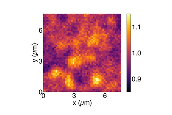
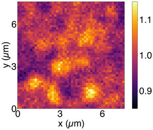
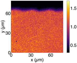
An array of squares, about 50 squares to a side, flicker constantly between lighter and darker colors, with many brighter blobs remaining more or less in the same location. In a few places, blobs noticeably blink on and seem to disappear afterward. The blobs seem to average 200 to 300 nanometers (4 to 6 squares) in diameter, with some larger and some smaller.
“The calculations that motivated us to look for this are actually pretty old. In the mid-2000s, people were predicting what they called a current channeling phenomenon,” said Chris Giebink, U-M professor of electrical and computer engineering and also senior author of the study. “You could liken it to a hilly landscape. The electrons, or charge carriers, that move through the device tend to want to follow the lowest energy pathways, so they’ll travel along the valleys.”
Charge carriers come in two flavors, electrons and positively charged “holes,” which run in opposite directions through the landscape. Where those rivers cross, light-emitting molecules convert electron-hole pairs into photons, or particles of light.
Because some valleys are deeper than others, they tend to support high-traffic rivers of charge carriers, with densities that are thought to be 10 to 100 times higher than the rest of the material. In contrast, crystalline materials are more uniform. Their landscape is flatter, leading the charge carriers to spread out more evenly, reducing the hotspot effect.
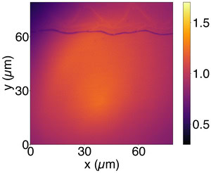
Theory suggests that the hotspots are just a few tens of nanometers across. They appear as graininess in images from an optical microscope, which is limited to details of a couple hundred nanometers or bigger.
“An initial concern was whether we were seeing a microscope artifact,” said Joshua Springsteen, a Ph.D. student in electrical and computer engineering and first author of the study. “We examined the same area of the device with our microscope using both photoluminescence and electroluminescence, confirming that it was an electrical phenomenon.”
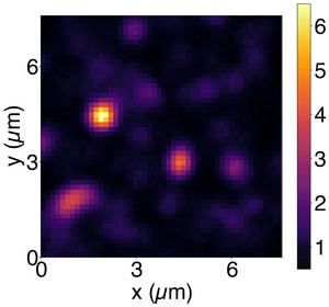
Because some of the lights flicker and aren’t always in sync, Springsteen could take a video of the device and run it through software that keyed in on the changes in brightness when one hotspot switched off while another stayed on. This technique, called superresolution optical fluctuation imaging, helped the team confirm that the hotspots were smaller than half the wavelength of the green light they emitted.
The researchers believe the blinking is due to charge carriers that are temporarily trapped in dips in the energy landscape. When that happens, they act more like dams, repelling other charge carriers, which seek alternate routes and cause downstream hotspots to go dark. Eventually, the charge carrier absorbs enough heat to pop back out of the dip, and the original hotspot lights up again. Because the flickering hotspots aren’t in sync, the human eye perceives amorphous OLEDs as glowing steadily.
To confirm that they had the mechanism right, the team used those earlier calculations that showed where charge-carrier rivers flow and meet. Springsteen took these theoretical freeze-frames and processed them to mimic the way the hotspots would have been blurred by the superresolution microscopy technique they used. These modified modeling images resembled the experimental images well enough that the team is confident they were seeing the hotspots.
The device was built in the Lurie Nanofabrication Facility and studied at the Michigan Center for Materials Characterization, both of which are operated and maintained with support from indirect cost allocations in federal grants.
The team has applied for patent protection with the assistance of U-M Innovation Partnerships and is licensed to Universal Display Corporation. Forrest and the University of Michigan have a financial interest in Universal Display Corporation.
Forrest is also the Paul G. Goebel Professor of Engineering and a professor of electrical and computer engineering, materials science and engineering, and physics. Giebink is also a professor of physics.