The “Magic Ratio” that could power tomorrow’s solar cells
A Q&A with Rachel Goldman
5 minutes
A Q&A with Rachel Goldman
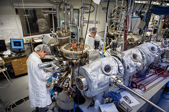
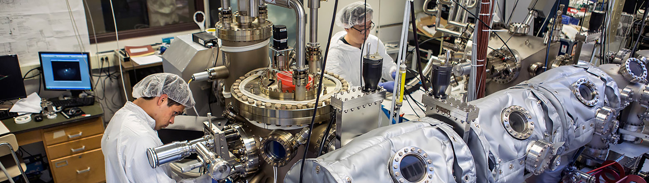
Rachel Goldman’s lab is working to produce “designer alloys” with carefully tailored electrical and light-absorbing properties. These materials could one day be used to build solar cells with double the efficiency of the flat-panel silicon cells that dot rooftops today. The new cells, called concentrator photovoltaics, use gallium arsenide semiconductors instead of the silicon-based semiconductors used in today’s cells. Gallium arsenide could move us toward the utility-scale solar arrays we’ll need to make solar energy a large part of our electrical infrastructure.
In her most recent paper, Goldman and her collaborators moved forward the science by figuring out how incorporating small fractions of nitrogen and bismuth in gallium arsenide semiconductors affects their structure and light-absorbing properties, creating a new map for bandgap engineering of designer semiconductor alloys. The advance could accelerate the development of concentrator photovoltaics, and could also lead to advances in semiconductor lasers and quantum computing.
Goldman is a professor of materials science and engineering. We sat down with her recently to learn more about her work.
Concentrator photovoltaics will depend on the development of alloys that are safer and less expensive than those currently used in gallium arsenide semiconductors. In our earlier research, we developed alloys that use a combination of nitrogen and bismuth. Since then, we’ve been working to develop a more complete understanding of exactly how the nitrogen-bismuth combination functions, and how changing the proportion of those two elements affects the alloy’s overall properties.
That research led us to the “magic ratio”—the precise proportion of bismuth to nitrogen that works best with a gallium arsenide substrate. We’ve found that by slightly tweaking that ratio within a certain range, we can control what bandwidth of light that the alloy absorbs.
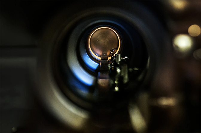
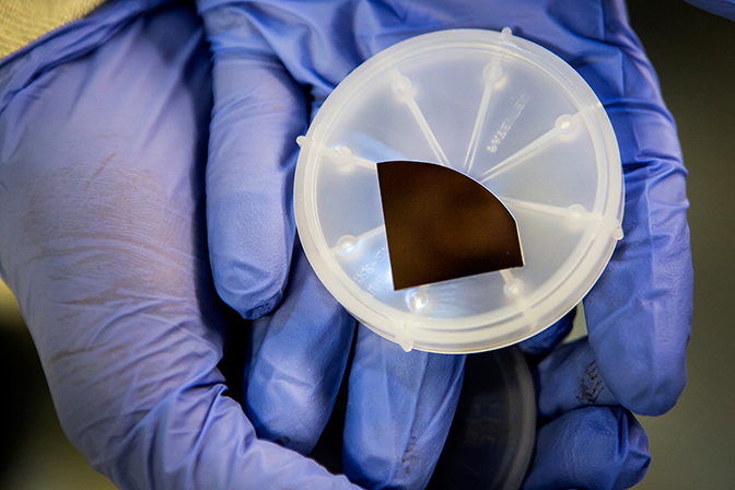
Turning “near-infrared” light into electricity is one big challenge—this is light that’s just outside the visible spectrum. A gallium arsenide solar cell consists of several thin layers of metal alloy sprayed onto a gallium arsenide substrate. It’s these thin layers that turn light into electrical charge. Each layer absorbs only a specific wavelength of light. A wavelength that slips through one layer can be caught by the next.
The “magic ratio” should help researchers dial in the exact mix of an alloy to absorb whatever bandwidth of light they choose.
We had to start by acknowledging that the conventional way of thinking about alloy composition doesn’t work for bismuth-nitrogen alloys.
Making an alloy out of individual atoms is a little like filling a box with a mix of differently-sized marbles. If you know the sizes of the marbles and the size of the box, you can calculate the combination of marbles that will fill the box exactly. Researchers can calculate the composition of most alloys by using x-ray diffraction to measure the “box” and then calculating the combination of atoms that fits.
That doesn’t work with bismuth and nitrogen. Bismuth is very large and nitrogen is very small, so it’s more like mixing sand and marbles. It’s hard to measure the size of a single grain of sand and even harder to predict how it will flow around all those marbles.
So we worked with labs in New Mexico, Poland and Romania, as well as here at U-M, to develop a series of measurements that would each solve part of the puzzle. Then we brought them all together to precisely determine the ratio of nitrogen to bismuth in a wide range of sample alloys, and how that ratio affects light absorption properties.
A better understanding of nitrogen-bismuth alloys could help us build more efficient infra-red lasers, which are widely used in fiber-optic communications and in the military. They could also be used in quantum computing, to build transistors that use the spin of electrons as a way to store information.
There’s still a lot of progress to be made. But this research opens the door to a better understanding of exactly how these alloys work and how to make them do what we want, in solar power and elsewhere.
Goldman’s most recent paper is titled “Mapping the composition-dependence of the energy bandgap of GaAsNBi alloys.” It is published in the August 23, 2019 issue of Applied Physics Letters. U-M graduate researcher Jordan Occena, T. Jen and J.W. Mitchell are also authors on the paper.
An earlier, related paper is titled “Bi-enhanced N incorporation in GaAsNBi alloys.” It published in the June 15, 2017 issue of Applied Physics Letters.