
Miniature and durable spectrometer for wearable applications
A team led by P.C. Ku and Qing Qu has developed a miniature, paper-thin spectrometer measuring 0.16mm2 that can also withstand harsh environments.
A team led by P.C. Ku and Qing Qu has developed a miniature, paper-thin spectrometer measuring 0.16mm2 that can also withstand harsh environments.
Researchers have developed a wafer-thin chip-scale spectrometer that is suitable for wearable applications. The robust gallium nitride lab-on-a-chip device can also withstand harsh environments with severe radiation, such as space exploration, or those with high temperatures – and can be adapted to do blood analysis by simply projecting light onto the skin. It measures a mere 0.16mm2.
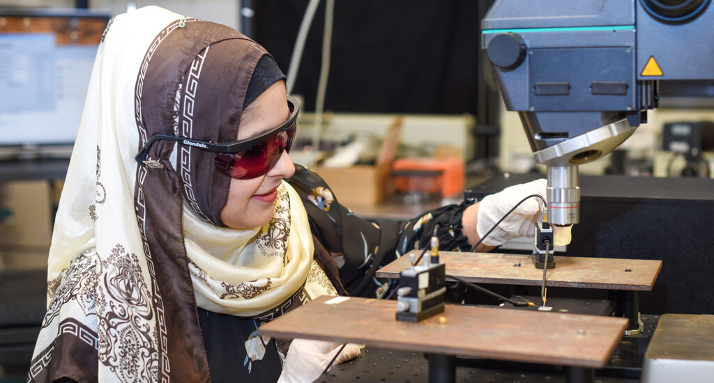
“As a wearable device, we’ll be able to put our device on a flexible substrate, such as sheets or fabric – or maybe on skin,” said doctoral researcher Tuba Sarwar.
A spectrometer uses spectroscopy to glean a wide range of information about a substance based on how it absorbs and reflects light. Optical spectroscopy, which measures an optical signal’s spectrum, is among the most prevalent method forms of spectroscopy. Specifically, it measures the relative spectral power density of the spectrum at different wavelengths.
The prototype optical spectrometer created by Sarwar and other members of Prof. P.C. Ku’s team was initially developed with a specific purpose: measuring an athlete’s sweat in a device that could be worn as a skin patch. This application was determined by U-M’s Exercise and Sport Science Initiative (ESSI). The device needn’t last long; in fact, being disposable was a plus.
Making such a device would require extreme miniaturization of current devices available in the marketplace, which measure closer to 12 cubic inches and cost hundreds to thousands of dollars. It would also require creating a device that can work in real time under changing conditions.
“Commercially, there are a lot of spectrometers that can work better than ours,” said Sarwar. “But our focus was miniaturization, especially the thickness of the device. These two features can give us an analysis of an active sample, such as sweat. We don’t need to go into the lab to use sophisticated instruments to get very precise measurements.”
Sarwar’s reference to a lab underscores the reality that most commercially available spectrometers require a bench top system consisting of several distinct optical elements: 1) a light source to excite the sample; 2) spectral encoders to translate the light from the sample into a readable output; and 3) photodetectors to translate the encoded signal into the spectrum.
Among these three elements, the spectral encoders often take up the most space or thickness which makes a thin sheet of spectrometer that can be suitable for epidermal applications difficult.
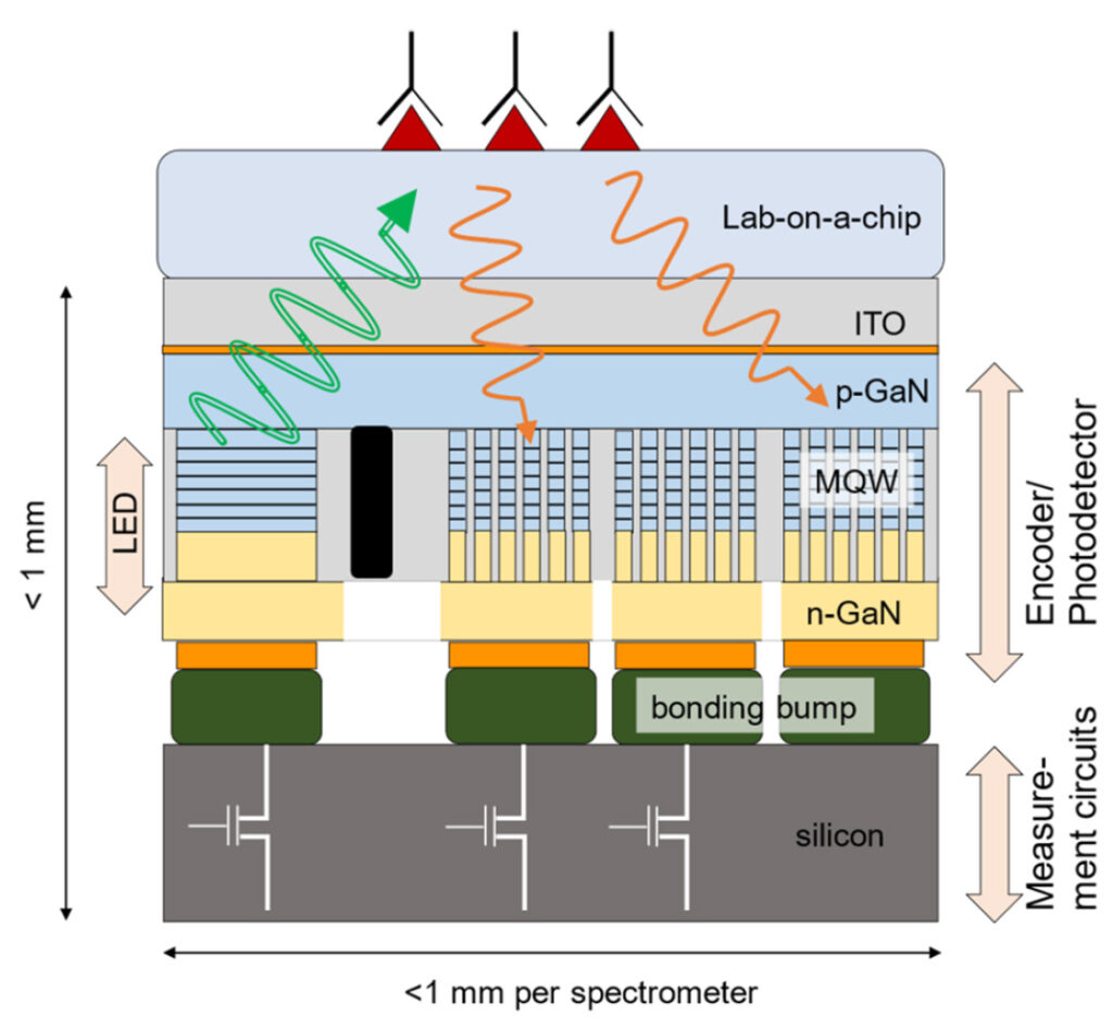
Ku, Qu, and their team took on the challenge of creating a device that could achieve ESSI’s goal, and created a miniaturized, low power, integrated device that works in visible light, specifically, within the wavelength range of 400-645nm.
The team’s spectrometer includes only 16 photodetectors, each responsive to a unique spectrum of the light. This low number of photodetectors was made possible by two key techniques.
First, the team used strain engineering on gallium nitride (GaN)-based spectral encoders. Strain engineering is a technique used, for example, in semiconductor manufacturing in which the material is stressed, or deformed. Done correctly, it can lead to new material properties that are better suited to specific applications. GaN semiconductors were selected as the foundational material because of their excellent optical properties across the visible spectrum.
The desired result of a dramatically reduced dependence on the angle of the light was accomplished, which eliminated the need for precise positioning of the spectrometer and the associated optics. It also allowed the photodetectors to reside alongside the spectral encoders on the same chip.
Second, the team incorporated machine learning into the device’s operation in order to decode the signal emitted from the detector. Doctoral researcher Can Yaras used a simple non-negative least-squares (NNLS) algorithm to enable an efficient computational algorithm to recover the spectral information from the detectors’ signal.
In terms of performance, the device was highly accurate in determining the peak wavelengths (with a standard deviation of 0.97%), but less accurate in measuring intensity ratio over different peak positions (with a standard deviation of 21.1%, or 10.4% after removing one outlier).
The team expects that the reading of intensity ratios can be improved by increasing the number of photodetectors, and further developing the machine learning algorithm, such as by applying deep learning techniques. They are also working on several other enhancements to the prototype spectrometer.
“Our goal was not to build the best spectrometer in the world in terms of the resolution,” said Ku, “but to focus on other aspects that are just as exciting if not more: the size, the thickness, the power consumption, and the ease of operation.”
In terms of future applications, Sarwar says that this miniature spectrometer could be built into a skin patch for health monitoring and diagnosis. The advantage it would have over existing devices is the fact that the excitation light source can also be easily integrated. The radiation hardness of the GaN semiconductors also makes the device potentially suitable for space exploration.
The device is described in Miniaturizing a Chip-Scale Spectrometer Using Local Strain Engineering and Total-Variation Regularized Reconstruction, by doctoral students Tuba Sarwar, Can Yaras, and Xiang Li, and professors Qing Qu and Pei-Cheng Ku, Nano Letters, October 12, 2022.
Work was performed in the Lurie Nanofabrication Facility. The research was supported by ESSI and the University of Michigan Blue Sky Initiative. The machine learning work was supported by NSF, ONR, and MIDAS.