Quantum tech: Semiconductor “flipped” to insulator above room temp
Discovery could pave the way to high speed, low-energy quantum computing.

Discovery could pave the way to high speed, low-energy quantum computing.
A semiconducting material that performed a quantum “flip” from a conductor to an insulator above room temperature has been developed at the University of Michigan. It potentially brings the world closer to a new generation of quantum devices and ultra-efficient electronics.
Observed in two-dimensional layers of tantalum sulfide only a single atom thick, the exotic electronic structure that supported this quantum flip was previously only stable at ultra-cold temperatures of -100 degrees Fahrenheit. The new material remains stable at up to 170 degrees Fahrenheit.
“We’ve opened up a new playground for the future of electronic and quantum materials,” said Robert Hovden, a U-M assistant professor of materials science and engineering and corresponding author on the paper in Nature Communications. “It represents a whole new way to access exotic states.”
Hovden explains that exotic quantum properties—like the ability to switch from a conductor to an insulator—could be key to the next generation of computing, providing more ways to store information and faster switching between states. That could lead to far more powerful and more energy-efficient devices.

Today’s electronics use tiny electronic switches to store data; ”on” is one and “off” is zero, and the data disappears when the power is turned off. Future devices could use other states, like “conductor” or “insulator” to store digital data, requiring only a quick blip of energy to switch between states rather than a steady stream of electricity.
In the past, however, such exotic behavior has only been observed in materials at super-cold temperatures. The ultimate goal is to develop materials that can quickly “flip” from one state to another on demand and at room temperature. Hovden says this research could be an important step in that direction.
“Previous research at ultra-cold temperatures has shown that it’s possible to make these kinds of flips happen on demand, over and over again,” he said. “That wasn’t the focus of this project, but the fact that we were able to keep even one flip stable at room temperature opens a lot of exciting possibilities.”
The flip from conductor to insulator is supported by a phenomenon called a charge density wave—an ordered, crystal-like pattern of positive and negative electrical charge that occurs spontaneously in certain conditions.
“Charge density waves have been observed before in bulk samples of tantalum sulfide, but the material had to be at ultra-cold temperatures,” Hovden said. “By interleaving several two-dimensional layers together, we were able to make it much more stable.”
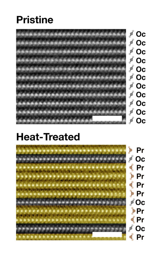
The team began by fabricating a sample of several single-atom-thick layers of tantalum sulfide sandwiched together. Each layer was a semiconductor in what’s called an octahedral state, which refers to a specific arrangement of tantalum and sulfur atoms. And while some charge density waves were present, they were too unstable and disordered to give rise to exotic behavior like a conductor-insulator flip.
Caption: This electron microscopy video shows layers of tantalum sulfide converting from octahedral to prismatic state during the heat-treating process. Video: Suk Hyun Sun, University of Michigan
But Suk Hyun Sung, a graduate researcher in Hovden’s lab and the first author on the paper, changed the sample’s properties by heating it in an oxygen-free environment while observing the process under an electron microscope. As the sample heated, layers began to switch, one by one, into a prismatic state—a different arrangement of the same atoms.
When most, but not all, layers had switched to prismatic state, Sung cooled the sample back to room temperature. He found that the layers that remained in the octahedral state were exhibiting charge density waves that were orderly and stable, and stayed that way at temperatures of up to 170 degrees Fahrenheit. In addition, those layers had flipped from semiconductors to insulators.
“Most 2D materials are subject to all the defects of whatever they’re sitting on, whatever’s in the air, and that makes them very unstable” Sung said. “But we discovered that when octahedral layers are nestled between several prismatic layers, they’re much more stable.”
The team is examining the phenomenon further, tweaking more variables of the process and testing mechanisms to control the exotic behaviors spurred by the charge density waves. For now, the new discovery has given them an important glimpse into the workings of quantum states and two-dimensional materials.
The work was performed in part at the U-M Lurie Nanofabrication Facility, and it includes contributions from researchers at Cornell University, the U.S. Naval Research Laboratory and the Chinese Academy of Sciences.
The research team also includes U-M materials science and engineering assistant professor John T. Heron; U-M assistant professor of electrical engineering and computer science Parag B. Deotare; U-M materials science and engineering graduate student researchers Steve Novakov, Xiangpeng Luo, Jiseok Gim and Nguyen Vu; U-M electrical engineering and computer science graduate student research assistant Zidong Li, U-M College of Literature, Science and the Arts Associate Professor of Physics Kai Sun; U-M College of Literature, Science and the Arts Assistant Professor of Physics Liuyan Zhao; Kavil Institute at Cornell for Nanoscale Science researcher Lena F. Kourkoutis; Cornell Department of Physics researcher Ismail El Baggari; U.S Naval Research Laboratory material science and technology researcher Todd Brintlinger; and Chinese Academy of Sciences Institute of Solid State Physics researchers Yu Liu, Wenjian Lu and Yuping Sun.