Mapping quantum structures with light to unlock their capabilities
Rather than installing new “2D” semiconductors in devices to see what they can do, this new method puts them through their paces with lasers and light detectors.
Rather than installing new “2D” semiconductors in devices to see what they can do, this new method puts them through their paces with lasers and light detectors.
A new tool that uses light to map out the electronic structures of crystals could reveal the capabilities of emerging quantum materials and pave the way for advanced energy technologies and quantum computers, according to researchers at the University of Michigan, the University of Regensburg and the University of Marburg.
A paper on the work is published in Science.
Applications include LED lights, solar cells and artificial photosynthesis.
“Quantum materials could have an impact way beyond quantum computing,” said Mackillo Kira, a professor of electrical engineering and computer science at the University of Michigan, who led the theory side of the new study. “If you optimize quantum properties right, you can get 100% efficiency for light absorption.”
Silicon-based solar cells are already becoming the cheapest form of electricity, although their sunlight-to-electricity conversion efficiency is rather low, about 30%. Emerging “2D” semiconductors, which consist of a single layer of crystal, could do that much better—potentially using up to 100% of the sunlight. They could also elevate quantum computing to room temperature from the near-absolute-zero machines demonstrated so far.
“New quantum materials are now being discovered at a faster pace than ever,” said Rupert Huber, a professor of physics at the University of Regensburg in Germany, who led the experimental work. “By simply stacking such layers one on top of the other under variable twist angles, and with a wide selection of materials, scientists can now create artificial solids with truly unprecedented properties.”
The ability to map these properties down to the atoms could help streamline the process of designing materials with the right quantum structures. But these ultrathin materials are much smaller and messier than earlier crystals, and the old analysis methods don’t work. Now, 2D materials can be measured with the new laser-based method at room temperature and pressure.
The measurable operations include processes that are key to solar cells, lasers and optically driven quantum computing. Essentially, electrons pop between a “ground state,” in which they cannot travel, and states in the semiconductor’s “conduction band,” in which they are free to move through space. They do this by absorbing and emitting light.
By simply stacking such layers one on top of the other under variable twist angles, and with a wide selection of materials, scientists can now create artificial solids with truly unprecedented properties.”
Rupert Huber, University of Regensburg professor of physics
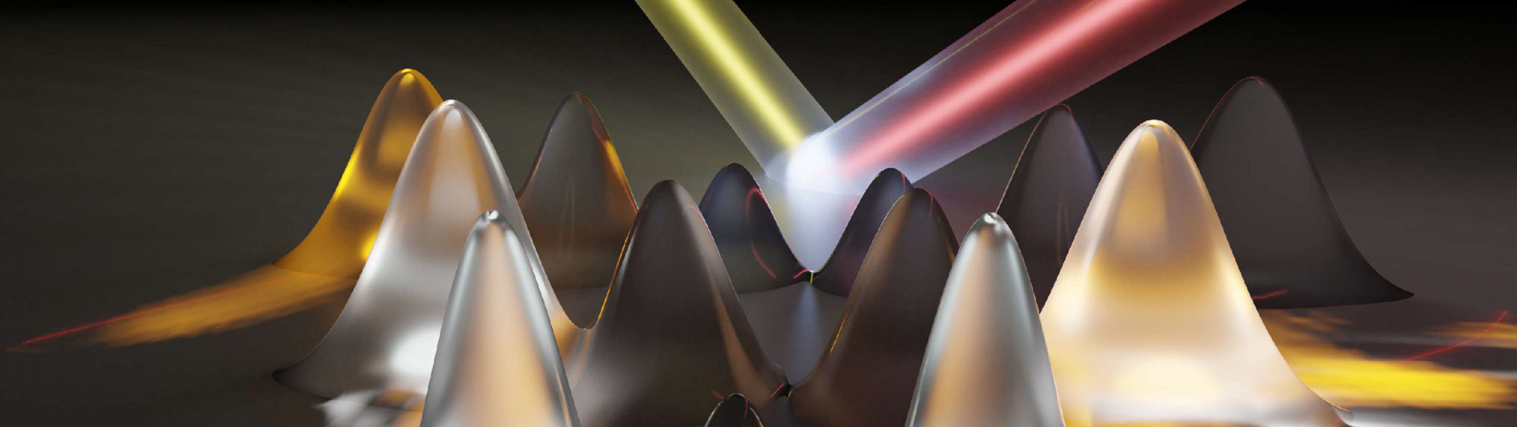
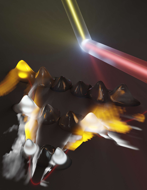
The quantum mapping method uses a 100 femtosecond (100 quadrillionths of a second) pulse of red laser light to pop electrons out of the ground state and into the conduction band. Next the electrons are hit with a second pulse of infrared light. This pushes them so that they oscillate up and down an energy “valley” in the conduction band, a little like skateboarders in a halfpipe.
The team uses the dual wave/particle nature of electrons to create a standing wave pattern that looks like a comb. They discovered that when the peak of this electron comb overlaps with the material’s band structure—its quantum structure—electrons emit light intensely. That powerful light emission along, with the narrow width of the comb lines, helped create a picture so sharp that researchers call it super-resolution.
By combining that precise location information with the frequency of the light, the team was able to map out the band structure of the 2D semiconductor tungsten diselenide. Not only that, but they could also get a read on each electron’s orbital angular momentum through the way the front of the light wave twisted in space. Manipulating an electron’s orbital angular momentum, known also as a pseudospin, is a promising avenue for storing and processing quantum information.
In tungsten diselenide, the orbital angular momentum identifies which of two different “valleys” an electron occupies. The messages that the electrons send out can show researchers not only which valley the electron was in but also what the landscape of that valley looks like and how far apart the valleys are, which are the key elements needed to design new semiconductor-based quantum devices.
For instance, when the team used the laser to push electrons up the side of one valley until they fell into the other, the electrons emitted light at that drop point too. That light gives clues about the depths of the valleys and the height of the ridge between them. With this kind of information, researchers can figure out how the material would fare for a variety of purposes.
The paper is titled, “Super-resolution lightwave tomography of electronic bands in quantum materials.” This research was funded by the Army Research Office, the German Research Foundation and the U-M College of Engineering Blue Sky Research Program. The Army Research Office is an element of the U.S. Army Combat Capabilities Development Command’s Army Research Laboratory.