Nanoparticles could spur better LEDs, invisibility cloaks
More efficient LED lighting and invisibility cloaking are two possible applications for a new process that adds metallic nanoparticles to semiconductors.
5 minutes
More efficient LED lighting and invisibility cloaking are two possible applications for a new process that adds metallic nanoparticles to semiconductors.
In an advance that could boost the efficiency of LED lighting by 50 percent and even pave the way for invisibility cloaking devices, a team of University of Michigan researchers have developed a new technique that peppers metallic nanoparticles into semiconductors.
The first technique that can inexpensively grow metal nanoparticles both on and below the surface of semiconductors, the process adds virtually no cost during manufacturing and its improved efficiency could allow manufacturers to use fewer semiconductors in finished products, making them less expensive.
The metal nanoparticles can increase the efficiency of LEDs in several ways. They can act as tiny antennas that alter and redirect the electricity running through the semiconductor, turning more of it into light. They can also help reflect light out of the device, preventing it from being trapped inside and wasted.
The process can be used with the gallium nitride that’s used in LED lighting and can also boost efficiency in other semiconductor products, including solar cells. It’s detailed in a paper published July 19 in Journal of Applied Physics.
“This is a seamless addition to the manufacturing process, and that’s what makes it so exciting,” said U-M materials science and engineering professor Rachel S. Goldman “The ability to make 3-D structures with these nanoparticles throughout is going to open a lot of possibilities.”
The idea of adding nanoparticles to increase LED efficiency is not new. But previous efforts to incorporate them have been impractical for large-scale manufacturing. They focused on pricey metals like silver, gold and platinum. In addition, the size and spacing of the particles must be very precise; this required additional and expensive manufacturing steps. Furthermore, there was no cost-effective way to incorporate particles below the surface.
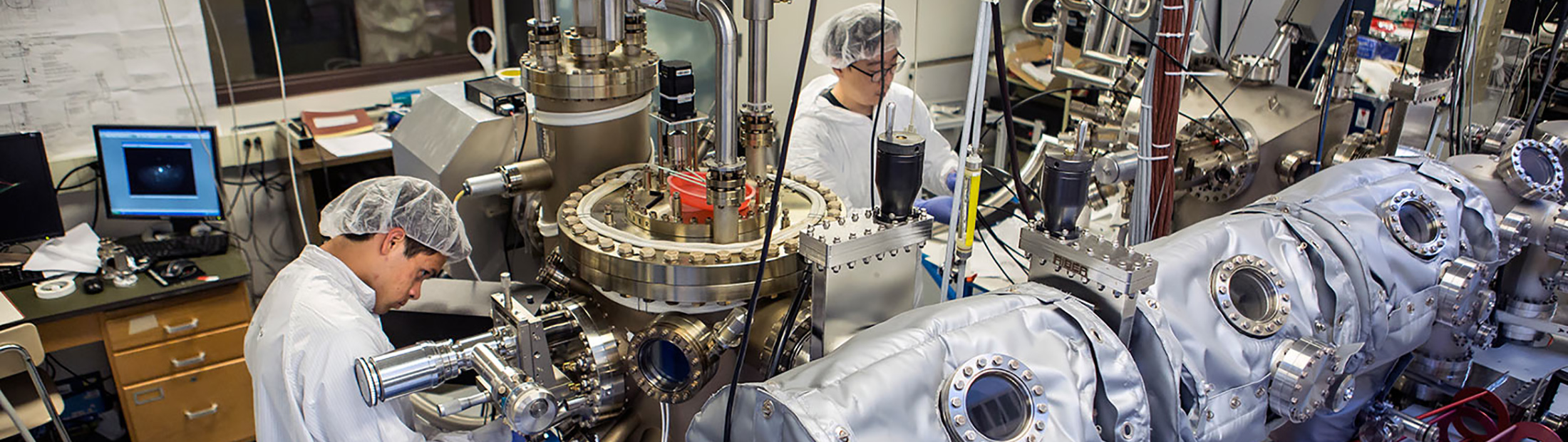
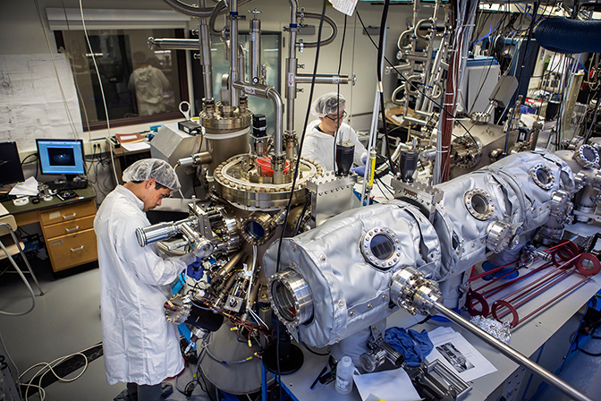
Goldman’s team discovered a simpler way that integrates easily with the molecular beam epitaxy process used to make semiconductors. Molecular beam epitaxy sprays multiple layers of metallic elements onto a wafer. This creates exactly the right conductive properties for a given purpose.
The researchers applied an ion beam between these layers—a step that pushes metal out of the semiconductor wafer and onto the surface. The metal forms nanoscale particles that serve the same purpose as the pricey gold and platinum flecks in earlier research. Their size and placement can be precisely controlled by varying the angle and intensity of the ion beam. And applying the ion beam over and over between each layer creates a semiconductor with the nanoparticles interspersed throughout.

“If you carefully tailor the size and spacing of nanoparticles and how deeply they’re embedded, you can find a sweet spot that enhances light emissions,” said Myungkoo Kang, a former graduate student in Goldman’s lab and the first author on the paper. “This process gives us a much simpler and less expensive way to do that.”
Researchers have known for years that metallic particles can collect on the surface of semiconductors during the manufacturing process. But they were always considered a nuisance, something that happened when the mix of elements was incorrect or the timing was off.
“From the very early days of semiconductor manufacturing, the goal was always to spray a smooth layer of elements onto the surface. If the elements formed particles instead, it was considered a mistake,” Goldman said. “But we realized that those ‘mistakes’ are very similar to the particles that manufacturers have been trying so hard to incorporate into LEDs. So we figured out a way to make lemonade out of lemons.”
Because the technique allows precise control over the nanoparticle distribution, the researchers say it may one day be useful for cloaks that render objects partially invisible by inducing a phenomenon known as “reverse refraction.”
Reverse refraction bends light waves backwards in a way that doesn’t occur in nature, potentially directing them around an object or away from the eye. The researchers believe that by carefully sizing and spacing an array of nanoparticles, they may be able to induce and control reverse refraction in specific wavelengths of light.
“For invisibility cloaking, we need to both transmit and manipulate light in very precise ways, and that’s very difficult today,” Goldman said. “This process could give us the level of control we need to make it work.”
The team is now working to adapt the ion beam process to the specific materials used in LEDs—they estimate that the higher-efficiency lighting devices could be ready for market within the next five years, with invisibility cloaking and other applications coming further in the future.
The paper is titled “Formation of embedded plasmonic Ga nanoparticle arrays and their influence on GaAs photoluminescence.” The research was supported by the National Science Foundation through the Materials Research Science and Engineering Center (MRSEC) at the University of Michigan, grant number DMR-1120923.