
CHIPS and Science Act: Implications and opportunities
The CHIPS and Science Act of 2022 promises to revitalize the U.S. semiconductor industry. Dennis Sylvester offers his perspective on what it means for ECE.

The CHIPS and Science Act of 2022 promises to revitalize the U.S. semiconductor industry. Dennis Sylvester offers his perspective on what it means for ECE.
The Creating Helpful Incentives to Produce Semiconductors (CHIPS) and Science Act of 2022, signed into law August 9, 2022, promises to bring relief to industries besieged by a chip shortage that has halted production of vehicles, consumer electronics, and much more. In anticipation of this historic initiative to revitalize the U.S. semiconductor industry, companies and educational institutions have already begun moving ahead with plans to maximize its impact.

Among those who have been planning far in advance of the signing of the CHIPS Act is Dennis Sylvester, Edward S. Davidson Collegiate Professor and Associate Chair of Electrical and Computer Engineering at the University of Michigan.
Sylvester is an internationally-recognized leader in the area of ultra-low power microprocessor design. He and his collaborators created the world’s smallest computer, called the Michigan Micro Mote (M3), much of which is currently being manufactured overseas. Ready to take advantage of the new opportunities presented by the signing of the CHIPS Act, Sylvester offers his perspective on this transformative event.
Why is there a CHIPS and Science Act?
The main goal of the Chips Act is to reignite semiconductor manufacturing in the United States, which has largely moved overseas. About $39B of the $52.7B budgeted over the next five years will be used for this purpose.
The current practice of designing chips, and then sending them to a large foundry to build them, began in the 1990’s and really took off in the 21st century. Companies moved to this so-called fabless model, or foundry model, as the cost of making more complicated chips in their own facilities became too expensive. The TSMC foundry in Taiwan emerged as a worldwide leader, and supply met demand for a number of years.
However, by 2020, the year the CHIPS Act was first introduced into Congress, many industries (and consumers) in the U.S. had been negatively impacted by a shortage of chips, making it both an economic and national security issue. The pandemic contributed to this shortage, as did an increasing demand for chips in general. The auto industry has been hit the hardest, followed by consumer electronics, and the list goes on (Goldman Sachs identified 169 industries negatively impacted by the chip shortage).
The CHIPS and Science Act will support a ramping-up of semiconductor foundries within the U.S. to meet this demand, and keep associated jobs in this country. The Act has already impacted a number of companies which have announced plans to invest billions of dollars to revamp their own chip manufacturing capabilities.
After the foundries, which are clearly the most expensive part, there are three primary areas of focus in the CHIPS Act: workforce development, core research, and translational activities, meaning moving technology from academia to industry.
How can ECE Departments contribute to workforce development?
ECE departments can play a big role in developing a workforce for the expanding semiconductor industry in the U.S., as can related disciplines such as materials science. For example, we can develop new courses, new certificate programs, and new degree specialties. We can also develop, or continue to offer, continuing education programs for those who are already working in an adjacent field and want to transition into this growing area.
One thing smaller departments in particular can do if they want to emphasize this as a growth area is to target specific semiconductor companies either locally or nationally and sponsor them at their career fairs, or invite them to come give a tech talk. Building this engagement could result in these companies inspiring and ultimately recruiting your students.
Looking beyond research 1-type universities, smaller colleges and even community colleges can become involved in training individuals for the expected job growth in this area. Many jobs at the foundries will be more technician oriented, and won’t require a master’s or Phd degree. But they will require specialized training in order to maintain the equipment, which are these big, huge, complex, laser-based or plasma-based devices.
One goal of the CHIPS Act is to bring jobs to more rural regions of the country. Intel has already announced that they are opening two new plants near Columbus, Ohio at an initial cost of $20B.
These foundries bring with them an entire ecosystem of supporting companies (and jobs) for activities such as packaging, testing, printed circuit board manufacturing, or even to just supply chemicals to the fabs. Many of those jobs are currently overseas as well.
What are some examples that Michigan has done to support workforce development in the semiconductor industry?
Michigan has always been strong in microelectronic and semiconductor research. We have among the largest number of graduate students in these fields in the country. And we have one of the finest cleanrooms in the country with the Lurie Nanofabrication Facility.
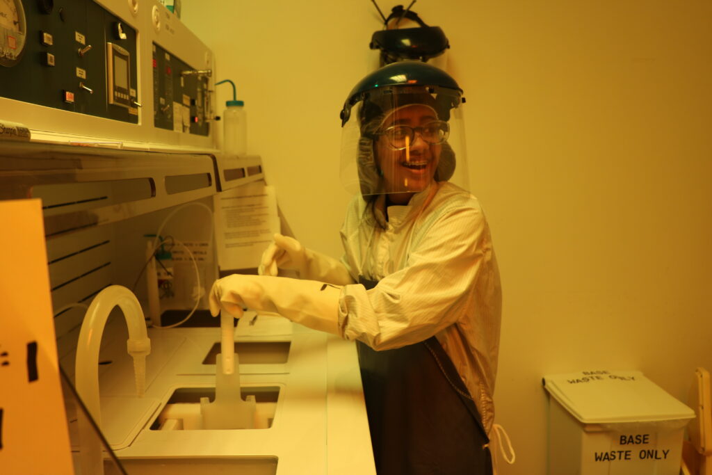
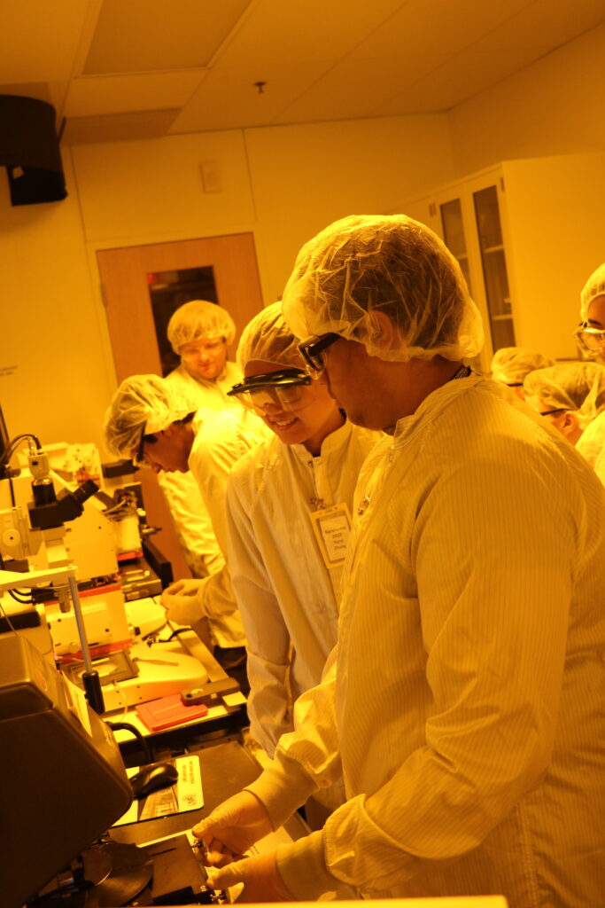
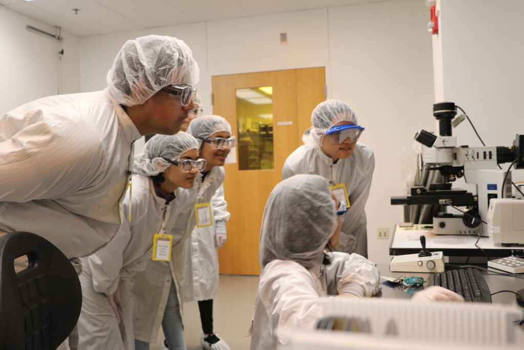
One of the things we’ve done in the past couple years is to overhaul and expand our core courses on semiconductor and MEMS fabrication that introduce senior level UG and first year grad students to the cleanroom. These classes train students from all kinds of disciplines to be able to understand how to use the equipment – what the work flow is like, what the bottlenecks are, and things like that.
I personally think just the act of getting students into a cleanroom to whet their appetite for this type of work is a great step toward helping increase the workforce in this area, even if they’re not going to be in a cleanroom or doing research in the area.
Summer is a great opportunity to reach out to younger students. We’ve done that with one of our research centers where we brought in STEM students from Detroit and other less advantaged areas to experience ECE research in general and the cleanroom in particular. We’ve done the same with one of our Electrify Tech Camps, though that’s been on hold the past couple years due to the pandemic.
My own research area is circuits, and there is a renewed push by companies to have students become more involved in the entire design and fabrication flow that they might see when they’re in industry. For example, Apple supported a design contest and a tape out class in my last class, and they’ve done this at other schools. In a future class, they’ll support fabrication of some of the chips if the students are willing to test them after getting them back.
This is similar to an in-class AMD Student Design Contest we had in previous years. Mike Flynn has done the same in two of his courses with support from Analog Devices and Apple. KLA has supported courses as well.
Our own students have taken the initiative to establish a Student Chapter of the IEEE Solid-State Circuits Society. Their goals include mentoring of younger students and fostering stronger relationships with industry. And our undergraduate student groups regularly invite companies to campus for Tech Talks.
To give you an idea of what we’ve done in terms of our graduate programs, we have a new master’s in engineering (MEng) program, with a specialty in microelectronics and IC design. The MEng program is designed for students who know what they want to do, and know they want to join industry when they graduate.
Can you comment on key aspects of the CHIPS Act as it pertains to research?
The CHIPS Act includes up to four microelectronics science research centers which are expected to be large collaborative efforts with significant funding. Details and RFPs should be coming out in the next few months. This is in addition to increased funding for microelectronics research in general, and specific research related to wireless technologies, energy innovation, clean water, and artificial intelligence for national security.
I also think that there are big growth opportunities for institutions looking to improve their infrastructure in this area, such as building a cleanroom, or improving their infrastructure in the physical sciences in general.
And how about the translational activities and industrial partnerships, which you stated was an additional major focus of the CHIPS Act?
The CHIPS and Science Act places a strong emphasis on moving from basic research to products that advance the state of microelectronics. If departments are not doing this already, they should probably make sure they highlight what they are doing in terms of moving innovations in research to the marketplace. At Michigan, ECE researchers are leaders among the entire university for generating translational research, as indicated by new U.S. patents, inventions, and startup companies. Many of our startup companies have grown out of research in the area of microelectronics, solid state and nanotechnology – all relevant to the semiconductor industry.
Some examples of forging stronger partnerships with industry have been already mentioned. The automotive industry is a huge customer for semiconductor manufacturing, as one example. And in this industry, there’s also lidars, radars, all kinds of optical or RF devices, sensors, as well as the interface circuits that are going into these cars. So there’s great potential for relationships being built to support these cool trends, which will also impact education as well as research.
Final thoughts?
The field of electrical and computer engineering has always been a leader in new technology and translational research. The CHIPS and Science Act is a huge opportunity for departments to capitalize on what they’re already doing, as well as sharpen their focus for the future.
Complete Bill and Division Summaries (U.S. Senate Committee on Commerce, Science, & Transportation)